Atomic Semi Rebrands as Fab2, Aims to Mass-Produce Small Chip Fabs
Jim Keller's latest venture, Atomic Semi, has rebranded as Fab2, explicitly signaling its ambitious mission to become a 'fab fab' – a factory dedicated to mass-producing small semiconductor fabrication plants.
✨ This content was summarized and interpreted by AI; it may contain errors — please verify accuracy with the original sources. Learn more
Listen to this story
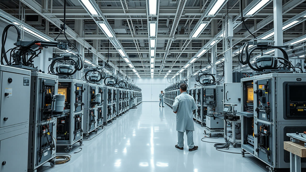
Jim Keller's latest venture, Atomic Semi, has officially rebranded as Fab2, explicitly signaling its ambitious mission to become a "fab fab" — a factory dedicated to mass-producing small semiconductor fabrication plants. This strategic shift underscores a radical approach to chip manufacturing, aiming to democratize access to advanced silicon production.
Founded by legendary chip architect Jim Keller and DIY fabrication pioneer Sam Zeloof, Fab2 is constructing a factory in Lockhart, Texas, specifically designed to churn out these smaller, self-contained fabs. The company has consolidated its operations in Texas, establishing a 120,000-square-foot headquarters in Austin for research and production, alongside its 30,000-square-foot "fab fab" in Lockhart. This move from its original California base marks a significant scaling of its physical footprint and operational focus.
The core innovation lies in Fab2's ability to design and build every tool within its fabs in-house, from pumps and valves to lithography equipment. These components are then assembled into machines, which in turn form complete, software-defined fabs. While utilizing electron-beam lithography for high resolution, this method is currently better suited for rapid prototyping and low-volume production rather than the high-throughput demands of commercial foundries. Fab2 also offers "Studio," an in-browser collaborative EDA tool to streamline chip design, complementing its hardware offering.
This "fab fab" model could profoundly impact the semiconductor industry by fostering decentralization and accelerating innovation. By making chip manufacturing more accessible and efficient, Fab2 aims to empower a new generation of hardware developers, potentially shortening development cycles from months to hours for specialized chips. However, scaling the throughput of electron-beam lithography will be crucial for wider commercial adoption beyond niche applications and rapid prototyping. The vision, backed by $15 million in seed funding for Atomic Semi, could redefine the landscape of chip production, moving towards a future where custom silicon is far more attainable.