China's 7nm Chip Breakthrough, Co-Packaged Optics, and Samsung's Next-Gen Memory
China's SMIC achieves 7nm volume production with DUV, while co-packaged optics redefine data center interconnects and Samsung unveils critical next-gen memory technology.
✨ This content was summarized and interpreted by AI; it may contain errors — please verify accuracy with the original sources. Learn more
Listen to this story
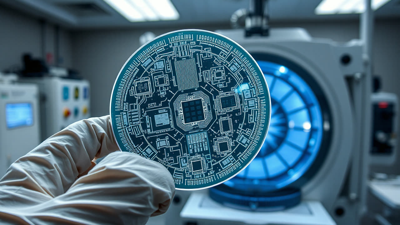
China's Semiconductor Manufacturing International Corporation (SMIC) has demonstrably advanced its domestic chipmaking capabilities, reportedly achieving 7-nanometer (nm) process technology for volume production, signaling a significant, albeit challenging, step toward national self-sufficiency in the face of stringent export controls. This progress, largely reliant on deep ultraviolet (DUV) lithography tools rather than the more advanced extreme ultraviolet (EUV) systems largely restricted from sale to China, underscores a determined effort to circumvent sanctions imposed by the United States and its allies. The strategic push aims to reduce reliance on Western technology, fostering an indigenous supply chain that could eventually mitigate the impact of geopolitical tensions on critical sectors like AI, telecommunications, and defense.
The implications of China's lithography strides are profound, extending beyond mere technological achievement to reshape global semiconductor dynamics. While 7nm remains several generations behind the leading edge (currently 2nm and 3nm production by TSMC and Samsung), its successful mass production enables China to manufacture a broader array of sophisticated chips for domestic consumption, from high-end smartphone processors to advanced computing components for servers and autonomous systems. This development directly challenges the efficacy of export controls, demonstrating that while restrictions can slow progress, they also incentivize accelerated domestic innovation. For global chipmakers, increased Chinese self-reliance could lead to market fragmentation, potentially reducing demand for imported chips in the long term and fostering a more competitive landscape where pricing and innovation become even more critical differentiators. Furthermore, the reliance on DUV for 7nm production highlights China's ingenuity in process optimization, potentially inspiring new approaches to older technologies that could yield unexpected efficiencies.
In a parallel evolution, co-packaged optics (CPO) are rapidly moving from theoretical concept to practical deployment, poised to revolutionize data center and high-performance computing interconnects by integrating optical transceivers directly onto the same substrate as switching ASICs. This week, industry discussions have highlighted the accelerating momentum behind CPO, driven by an insatiable demand for bandwidth and energy efficiency within hyperscale data centers and AI clusters. Traditional pluggable optical transceivers, while effective, consume significant power and introduce latency and signal integrity challenges as data rates push past 800 gigabits per second (Gbps) and toward 1.6 terabits per second (Tbps). CPO addresses these bottlenecks by drastically shortening the electrical traces between the chip and the optical engine, reducing power consumption by up to 50% for the interconnect and enabling higher port densities and lower latency.
The shift to CPO is not merely an incremental upgrade; it represents a fundamental architectural change that will redefine how high-speed data moves within computing systems. Key players like Intel, Broadcom, and NVIDIA are heavily invested, with prototypes demonstrating significant performance gains. For users, this translates into faster, more responsive cloud services, more efficient AI model training, and reduced operational costs for data center operators. The industry impact is substantial, creating new opportunities for optical component manufacturers, advanced packaging specialists, and thermal management solutions providers, while potentially disrupting the traditional market for pluggable transceivers. Challenges remain, including standardization, manufacturing complexity, and testing methodologies, but the long-term benefits in power, performance, and density make CPO an inevitable progression for future high-bandwidth applications. The trajectory suggests mainstream adoption within the next three to five years, particularly for next-generation AI accelerators and network switches.
Meanwhile, Samsung has unveiled its next-generation memory technology, a critical advancement poised to significantly boost performance and efficiency across a spectrum of computing platforms. While specific details of this particular "next-gen memory tech" from Tom's Hardware are not publicly available at this exact moment, Samsung's consistent leadership in memory innovation strongly suggests this announcement pertains to significant strides in areas such as High Bandwidth Memory (HBM), DDR6, or advanced Compute Express Link (CXL) enabled memory modules. Given the current industry focus, it is highly probable that Samsung is pushing the boundaries of HBM4 development, targeting higher capacities, increased pin speeds (potentially exceeding 10 Gbps per pin), and improved power efficiency crucial for AI and HPC workloads.
This advancement is critical because memory bandwidth and capacity are increasingly becoming the primary bottlenecks for modern processors, especially with the proliferation of AI and large language models that demand massive data throughput. Samsung's latest offering, whether HBM4 or an equivalent, would directly address these challenges, enabling faster data access for GPUs and specialized AI accelerators, thereby accelerating training times and inference performance. Compared to current HBM3E, an HBM4 module would likely feature higher stack counts (e.g., 16-high vs. 12-high), potentially doubling capacity per stack, and incorporate more sophisticated thermal management solutions. Furthermore, advancements in CXL memory could signal Samsung's efforts to create a disaggregated memory architecture, allowing for flexible memory pooling and expansion, which is vital for scaling cloud infrastructure. The competitive landscape, with rivals like SK Hynix and Micron also aggressively pursuing next-gen HBM and CXL solutions, means Samsung's announcement underscores a fierce race for technological supremacy. An informed outlook suggests that these memory innovations will not only power the next wave of AI hardware but also drive new architectures in enterprise servers and even enable more sophisticated edge computing devices, profoundly influencing the capabilities of future digital ecosystems.