Chipmakers Embrace ASML's High-NA EUV Machines, Eye 40% Productivity Boost
Leading chipmakers commit to ASML's $400 million High-NA EUV lithography machines and a pivotal process alteration, promising a 40 percent productivity amplification for advanced chip manufacturing.
✨ This content was summarized and interpreted by AI; it may contain errors — please verify accuracy with the original sources. Learn more
Listen to this story
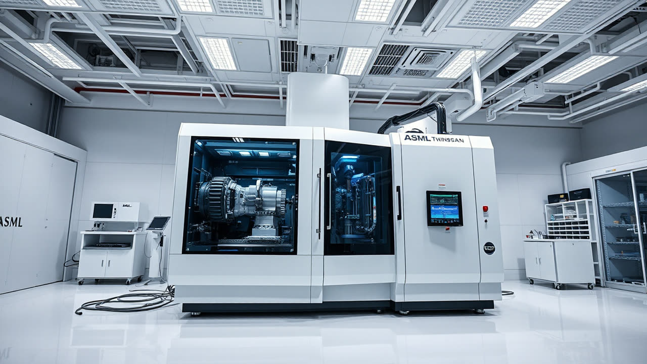
The semiconductor industry is poised for a monumental leap as leading chipmakers commit to ASML's groundbreaking $400 million High-NA extreme ultraviolet (EUV) lithography machines, alongside a pivotal process alteration projected to amplify their productivity by an astounding 40 percent. This agreement, coming as early adopters like Intel and TSMC prepare to integrate these advanced systems, signals a definitive shift in the economics and capabilities of advanced chip manufacturing, promising a new era of unprecedented transistor density and performance.
The core of this transformation lies with ASML's Twinscan EXE:5200 High-NA EUV scanner, a behemoth capable of printing features with a numerical aperture (NA) of 0.55, a significant upgrade from the 0.33 NA of current generation EUV systems. This enhanced NA allows for a finer resolution, enabling chipmakers to shrink transistor sizes further and pack more processing power onto a single die. The initial investment is substantial, with each machine costing approximately $400 million, a price tag that underscores the technological complexity and strategic importance of these tools. Intel, for instance, has already secured the first production High-NA EUV system, the Twinscan EXE:5000, installed at its Oregon facility, with plans for the EXE:5200 to follow, targeting its Intel 18A process node for production by 2025. TSMC and Samsung are also confirmed to be acquiring these machines, though their deployment timelines might vary slightly.
The "crucial chipmaking change" that unlocks the 40 percent productivity boost is centered around optimizing the patterning process itself. While specific details remain proprietary, industry analysts suggest this likely involves advancements in multi-patterning techniques, improved resist materials, and potentially novel mask designs or exposure strategies that minimize overhead and maximize wafer throughput per hour on the High-NA systems. For previous generations of EUV, double patterning was often discussed for features below a certain size. With High-NA EUV, the goal is to achieve single exposure patterning for even finer features, reducing complexity and manufacturing steps. This efficiency gain is not merely incremental; it fundamentally alters the return on investment for these incredibly expensive machines, making the pursuit of sub-2nm process nodes more economically viable. Without this productivity enhancement, the sheer cost per wafer might have made the widespread adoption of High-NA EUV prohibitive for many applications.
The implications for the industry are profound. For users, this translates directly into more powerful, energy-efficient, and compact devices. The ability to push transistor density further enables innovations across artificial intelligence, high-performance computing, advanced mobile platforms, and specialized accelerators. Chips manufactured with High-NA EUV will be the bedrock for the next generation of technological breakthroughs, driving performance improvements that would be unattainable with current lithography techniques. For chipmakers, the adoption of High-NA EUV is not merely an upgrade; it's a competitive imperative. Companies that successfully master this technology will gain a significant lead in the race to deliver the most advanced semiconductors, potentially dictating market share for years to come. The capital expenditure required, however, also raises the barrier to entry, further consolidating the market among a few well-resourced players.
Comparing High-NA EUV to its predecessor, Low-NA EUV (0.33 NA), reveals a generational leap rather than a mere iteration. Low-NA EUV, which became mainstream around 2019, enabled the production of 7nm and 5nm nodes, providing a critical path beyond the limitations of deep ultraviolet (DUV) lithography. High-NA EUV, with its 0.55 NA, roughly doubles the resolution, allowing for features to be scaled down to approximately 8 nanometers in half-pitch, compared to the 13 nanometer half-pitch of current EUV systems. This increased resolution directly translates into smaller transistors and denser circuits, essential for achieving 2nm and even 1.8nm (or Intel's 18A) process nodes. While Low-NA EUV required techniques like self-aligned double patterning (SADP) or self-aligned quadruple patterning (SAQP) for the most aggressive features, High-NA EUV aims to achieve these features with single exposure, simplifying the manufacturing process and reducing defect rates. The transition, however, is not without its challenges, including the need for new resist materials, more precise mask manufacturing, and extremely tight control over the entire lithography process.
Looking ahead, the widespread deployment of High-NA EUV systems, particularly with the confirmed productivity enhancements, will accelerate the industry's roadmap towards sub-2nm processes. While Intel is aggressively pursuing an early lead, TSMC and Samsung are expected to follow closely, ensuring a competitive landscape at the bleeding edge of chip manufacturing. We can anticipate the first commercial products leveraging High-NA EUV to emerge by late 2025 or early 2026, initially in high-value, performance-critical applications. The long-term outlook suggests a sustained period of innovation driven by these machines, pushing the boundaries of Moore's Law further than many had predicted just a few years ago. However, the immense cost and technical complexity will also spur greater collaboration between ASML, its suppliers, and the leading chipmakers, fostering an ecosystem where shared challenges lead to collective breakthroughs. The focus will inevitably shift to optimizing the entire manufacturing flow around these powerful new tools, from design methodologies to metrology and inspection, ensuring that the full potential of High-NA EUV is realized.