Intel Ships First High-Volume Chips Using ASML's High NA EUV Lithography
Intel becomes the first company to deploy ASML's advanced High Numerical Aperture Extreme Ultraviolet (High NA EUV) lithography in high-volume manufacturing for its Core Ultra Series 3 'Panther Lake' processors, marking a significant industry milestone.
✨ This content was summarized and interpreted by AI; it may contain errors — please verify accuracy with the original sources. Learn more
Listen to this story
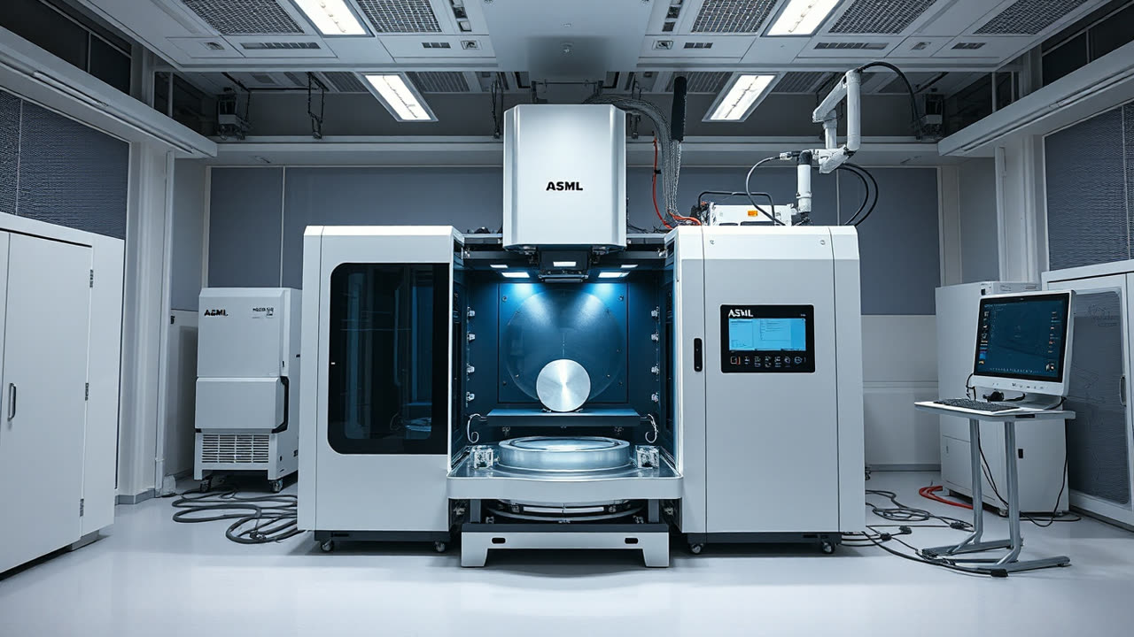
Intel Foundry has commenced shipping high-volume logic chips, specifically a subset of its Core Ultra Series 3 "Panther Lake" processors, utilizing ASML's cutting-edge High Numerical Aperture (High NA) Extreme Ultraviolet (EUV) lithography technology. This marks a pivotal moment for the semiconductor industry, as Intel becomes the first company to deploy High NA EUV in high-volume manufacturing, moving the advanced patterning technology beyond research and development.
The milestone involves select layers of Intel's 18A process node for Panther Lake, which are now dual-qualified for both existing 0.33 NA NXE scanners and the new 0.55 NA EXE scanners, demonstrating matched yields. This adoption of ASML's EXE:5000 and EXE:5200B systems underscores a significant leap in chip manufacturing capabilities. High NA EUV’s 0.55 numerical aperture, a substantial increase over standard EUV’s 0.33 NA, enables the printing of features 1.7 times smaller and achieves nearly three times higher transistor density in a single exposure. This enhanced resolution helps overcome the complexities and costs associated with multi-patterning techniques required by previous generations, promising improved process control and potentially faster production cycles.
For Intel, this achievement is a crucial validation of its "IDM 2.0" strategy, which aims to restore manufacturing leadership and offer advanced foundry services. Panther Lake, built on the 18A process featuring RibbonFET gate-all-around transistors and PowerVia backside power delivery, represents Intel's commitment to pushing the boundaries of silicon technology. While competitors like TSMC are reportedly delaying high-volume High NA EUV adoption due to the hefty investment (machines cost up to $400 million) and ongoing optimization of existing low-NA EUV, Intel's early integration could provide a strategic advantage in the race for next-generation chip performance and density, particularly for AI-driven applications. The real test now lies in the broader economic justification and widespread implementation of this expensive yet transformative technology across the industry.