Kioxia and Western Digital Unveil BiCS10: World's Highest-Density 3D QLC NAND Flash
Kioxia and Western Digital introduce BiCS10, a groundbreaking 3D QLC NAND flash memory with an unprecedented 332 active layers, 4,800 MT/s interface, and record areal density exceeding 37 Gbit/mm², fundamentally advancing storage capabilities.
✨ This content was summarized and interpreted by AI; it may contain errors — please verify accuracy with the original sources. Learn more
Listen to this story
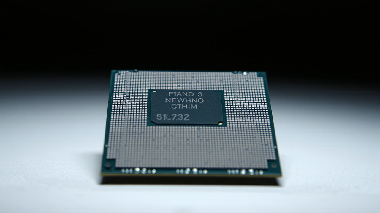
Kioxia and Western Digital (SanDisk's parent company) have unveiled BiCS10, a groundbreaking 3D QLC NAND flash memory featuring an unprecedented 332 active layers, an interface speed of up to 4,800 MT/s, and a record areal density exceeding 37 Gbit/mm². This significant technological leap, demonstrated at the 2024 Flash Memory Summit, represents a critical advancement in flash storage, pushing the boundaries of density and performance in a single package.
This development matters profoundly for both consumers and the enterprise storage industry, fundamentally altering the economics and capabilities of solid-state drives (SSDs). For users, the immediate impact will be the potential for even higher capacity SSDs at more accessible price points. QLC (Quad-Level Cell) NAND stores four bits per cell, inherently offering greater density than TLC (Triple-Level Cell) or MLC (Multi-Level Cell) NAND, albeit traditionally at the cost of endurance and performance. BiCS10's massive layer count and increased areal density amplify this advantage, enabling single SSDs to reach capacities previously only seen in traditional hard disk drives, making multi-terabyte drives commonplace and more affordable for mainstream desktops, laptops, and gaming consoles. The enhanced interface speed of 4,800 MT/s also ensures that these high-capacity drives can maintain competitive read and write performance, mitigating some of the traditional speed compromises associated with QLC technology.
For the industry, BiCS10's introduction underscores a continued reliance on vertical scaling to overcome the physical limitations of planar NAND. As lithography shrinks become increasingly challenging and expensive, stacking more layers becomes the most viable path to increasing bit density per wafer. This innovation allows manufacturers to produce more gigabytes per wafer, driving down the cost per bit and intensifying price competition in the SSD market. Data centers, in particular, stand to benefit immensely from BiCS10. The ability to pack more storage into a smaller physical footprint translates directly into reduced operational costs, including power consumption, cooling, and rack space. While enterprise-grade storage often demands higher endurance, the sheer density and improving performance of advanced QLC solutions like BiCS10 make them increasingly attractive for read-intensive workloads, archival storage, and cold data tiers where cost per gigabyte is paramount.
Comparing BiCS10 to its predecessors and rivals highlights its competitive edge. Kioxia and Western Digital's previous generation, BiCS9, typically featured around 218 active layers and offered lower interface speeds. The jump to 332 layers in BiCS10 signifies a substantial 50% increase in vertical stacking, directly translating to higher bit density per die. In the competitive landscape, Samsung's latest V-NAND generations have reached 236 active layers, with their eighth generation offering a 3,200 MT/s interface speed, while Micron's 232-layer 3D NAND also features a 2,400 MT/s interface. YMTC's Xtacking 3.0 technology has demonstrated 232 layers and an I/O speed of up to 2,400 MT/s. BiCS10's 332 layers and 4,800 MT/s interface clearly position it at the forefront in both layer count and raw interface bandwidth among publicly announced technologies, demonstrating Kioxia and Western Digital's aggressive push in NAND innovation. The areal density of over 37 Gbit/mm² is a particularly striking metric, showcasing superior efficiency in utilizing silicon space compared to prior generations and competitors.
Looking ahead, the introduction of BiCS10 suggests a clear trajectory for NAND flash development. The race for higher layer counts will undoubtedly continue, with manufacturers likely targeting the 400-layer mark and beyond in subsequent generations. We can anticipate further refinements in QLC technology, including improved error correction codes, more sophisticated controllers, and potentially even 5-bit-per-cell (PLC) NAND, to further enhance endurance and performance for broader application. The increased interface speeds, exemplified by BiCS10's 4,800 MT/s, will necessitate corresponding advancements in SSD controller technology and host interfaces like PCIe Gen5 and future Gen6 to fully harness the raw bandwidth. This trend will not only drive down SSD costs but also accelerate the transition away from traditional hard drives in an even wider range of applications, from personal computing to edge devices and the vast infrastructure of cloud computing. The sustained innovation in 3D NAND, particularly in QLC, ensures that storage density will continue its exponential growth, empowering new applications and making vast amounts of data more manageable and accessible than ever before.