Samsung Unveils Next-Gen Wafer-Bonded Memory for AI Data Centers
Samsung has introduced zHBM, zNAND-O, and BV-NAND, three advanced memory technologies leveraging wafer bonding to address the escalating demands of AI, machine learning, and high-performance computing.
✨ This content was summarized and interpreted by AI; it may contain errors — please verify accuracy with the original sources. Learn more
Listen to this story
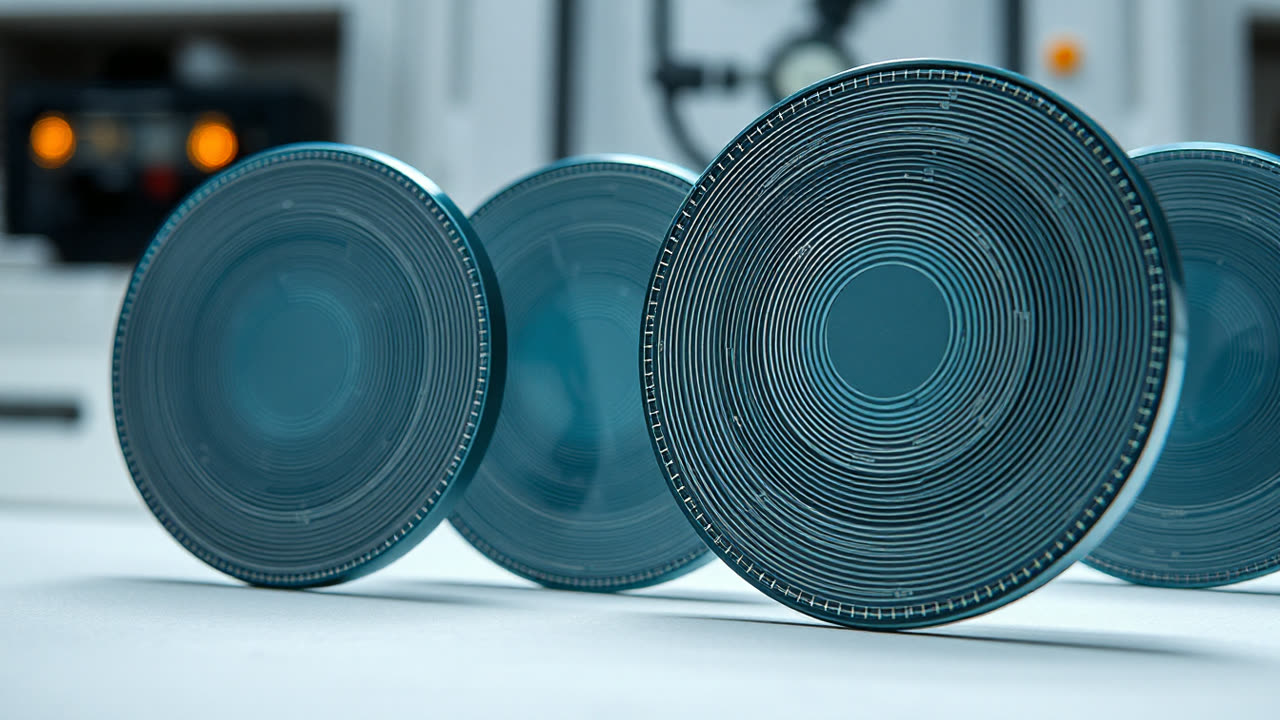
Samsung's recent unveiling of three distinct, next-generation memory technologies – zHBM, zNAND-O, and BV-NAND – marks a pivotal moment for AI data center architecture, fundamentally leveraging advanced wafer bonding techniques to push beyond existing performance and capacity ceilings. These innovations, showcased at the Flash Memory Summit (FMS), are not mere incremental upgrades but represent strategic plays designed to address the escalating memory demands of artificial intelligence, machine learning, and high-performance computing workloads.
The most striking development is zHBM, a formidable evolution in high-bandwidth memory that promises to redefine the throughput capabilities of AI accelerators. While specific performance benchmarks remain under wraps for commercial release, zHBM is engineered to surpass the bandwidth and capacity limitations of current HBM3E solutions, which already deliver over 1.2 TB/s per stack. This leap is critical because the performance bottleneck in many AI training and inference tasks has shifted from computational power to memory bandwidth and capacity. Large language models (LLMs) and complex neural networks demand massive datasets to be accessed simultaneously by hundreds or thousands of processing cores. zHBM, by allowing more data to flow to and from the processing units at unprecedented speeds, directly translates into faster model training, quicker inference times, and the ability to deploy larger, more sophisticated AI models without compromising latency. Its impact extends beyond raw speed, fostering a new generation of AI chips that can integrate significantly more memory, enabling on-chip processing of entire model parameters or larger context windows, thereby reducing reliance on slower off-chip storage.
Complementing zHBM in the memory hierarchy is zNAND-O, a novel offering positioned to bridge the substantial performance gap between DRAM and traditional NAND flash. While DRAM provides ultra-low latency and high bandwidth, its cost and volatility make it unsuitable for large-scale, persistent storage. Conventional NAND, conversely, offers high capacity at a lower cost but suffers from significantly higher latency and lower endurance. zNAND-O leverages wafer bonding to achieve a new class of non-volatile memory that delivers significantly improved read/write speeds and endurance compared to enterprise SSDs, albeit not reaching DRAM levels. This technology is poised to become a critical component in AI data centers for warm data storage, acting as a high-performance caching layer or persistent memory for frequently accessed model weights, intermediate results, and large datasets that require faster access than traditional NVMe SSDs can provide but are too large or costly for DRAM. It offers a cost-effective alternative to expensive, high-endurance SSDs for specific AI workloads, optimizing total cost of ownership while enhancing overall system responsiveness.
The third pillar of Samsung's announcement, BV-NAND (Bonded Vertical NAND), focuses on dramatically increasing the density and performance of NAND flash storage. By employing advanced wafer bonding, Samsung can stack multiple layers of NAND dies with unprecedented precision and interconnectivity, effectively creating a monolithic 3D structure that overcomes the physical limitations of traditional 3D NAND fabrication. This allows for significantly higher bit densities, meaning more storage capacity in a smaller footprint, and potentially lower manufacturing costs per bit. For AI, BV-NAND is crucial for cold and archival data storage, as well as for storing the massive foundational models and training datasets that underpin modern AI. The ability to pack petabytes of data into ever-smaller physical spaces while maintaining acceptable read speeds is vital for scaling AI infrastructure, reducing power consumption, and lowering the operational expenses associated with managing vast data lakes.
These innovations collectively underscore a strategic pivot in memory manufacturing, where advanced wafer bonding emerges as the unifying technological backbone. Wafer bonding allows for the direct connection of multiple wafers at a molecular level, enabling denser interconnections, reduced signal paths, and improved power efficiency compared to traditional packaging methods. This technique is not just about stacking; it's about creating heterogeneous integration, allowing different types of chips or functionalities to be combined seamlessly, opening doors for future memory-logic integration. While other memory manufacturers like SK Hynix and Micron are also advancing their HBM offerings and exploring novel NAND architectures, Samsung's simultaneous debut of three distinct, wafer-bonded memory types positions it as a leader in leveraging this foundational manufacturing shift across the entire memory spectrum.
Looking ahead, the immediate future will see zHBM integrated into next-generation AI accelerators from leading chipmakers, likely appearing in commercial products within the next 12-18 months. Its widespread adoption will be contingent on manufacturing yields and cost-effectiveness compared to established HBM3E. zNAND-O's trajectory is likely to involve niche deployments in high-end enterprise storage arrays and specialized AI servers, gradually expanding as its cost-performance ratio becomes more attractive. BV-NAND, with its focus on density, will likely see quicker integration into enterprise SSDs and large-scale data center storage solutions, driving down the cost of storing massive AI datasets. The success of these technologies will not only solidify Samsung's position in the fiercely competitive memory market but also catalyze a new wave of innovation in AI hardware, enabling models of unprecedented scale and complexity, further accelerating the pace of AI development and deployment across industries.