SK hynix Reveals HBM AI Memory Hits Physical 775-Micron Ceiling, Pushing Hybrid Bonding for HBM5
SK hynix announced at Hot Chips 2026 that HBM for AI faces a critical 775-micron thickness limit, necessitating a pivot to hybrid bonding for HBM5 and beyond, while extending MR-MUF for immediate solutions.
✨ This content was summarized and interpreted by AI; it may contain errors — please verify accuracy with the original sources. Learn more
Listen to this story
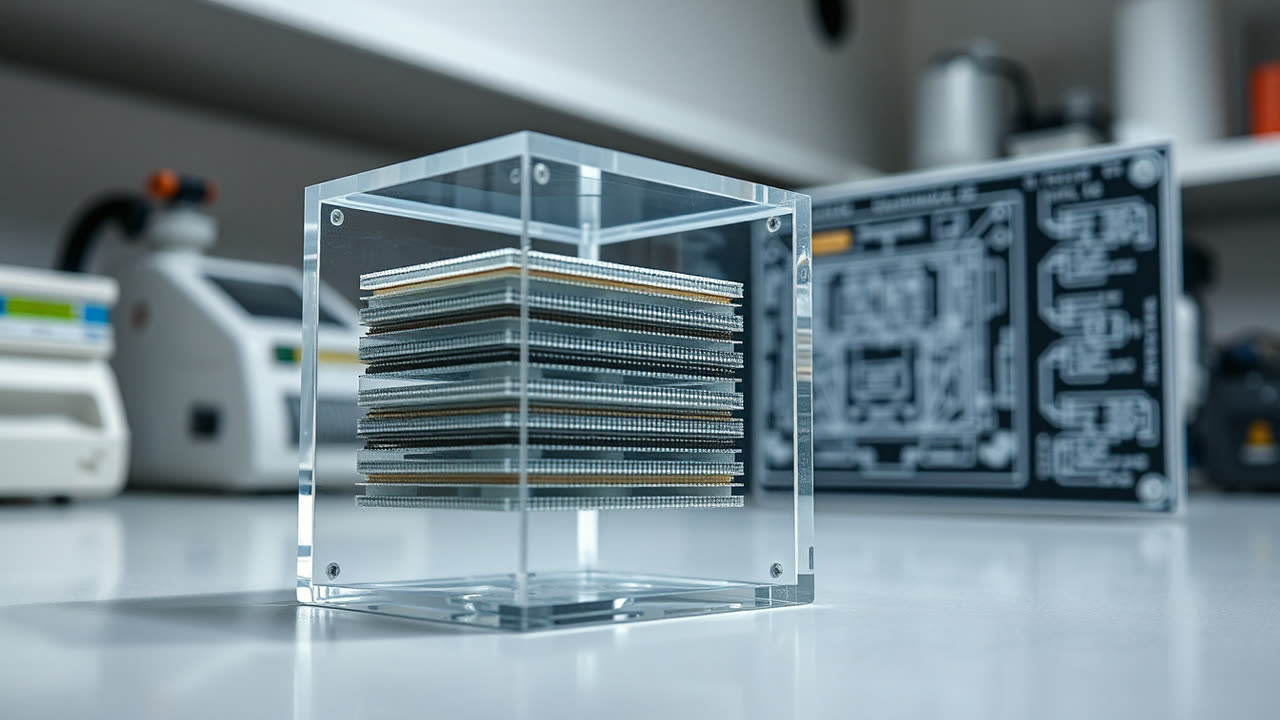
SK hynix has revealed at Hot Chips 2026 that the relentless pursuit of higher capacity and bandwidth in High Bandwidth Memory (HBM) for artificial intelligence applications is confronting a fundamental physical barrier: a 775-micron thickness ceiling for HBM cubes, directly constrained by the standard thickness of a 300mm logic wafer. This critical limitation, driven by co-packaging requirements with advanced AI accelerators, is compelling the industry to pivot towards next-generation manufacturing methodologies, with SK hynix championing hybrid bonding as the essential technology for HBM5 and beyond, even as it extends its current Mass Reflow Molded Underfill (MR-MUF) process for immediate solutions, notably through its collaboration on Nvidia's Rubin platform.
This 775-micron cap, a seemingly innocuous engineering specification, carries profound implications for the future of AI infrastructure. Current HBM designs, such as HBM3E and anticipated HBM4 variants, stack multiple DRAM dies vertically, interconnected by Through-Silicon Vias (TSVs) and encapsulated with various bonding and underfill techniques. As the number of stacked dies increases to meet the insatiable demand for memory capacity—with 12-high and even 16-high stacks on the horizon—the cumulative thickness of these dies, along with their interposers and bonding materials, quickly approaches and breaches this 775-micron threshold. Exceeding this limit complicates the integration of HBM stacks onto the same package substrate as the GPU or AI accelerator, potentially leading to thermal management challenges, increased manufacturing complexity, and even mechanical stress issues. The imperative for thinner dies and more efficient bonding becomes paramount to maintain the desired form factor and thermal envelope of future AI chips.
SK hynix's strategic push for hybrid bonding in HBM5 represents a significant technological leap designed to circumvent these physical constraints. Unlike traditional thermo-compression bonding (TCB) or the company's current MR-MUF process, which relies on micro-bumps and underfill materials, hybrid bonding directly fuses metal pads and dielectric layers between wafers at the atomic level. This advanced technique promises significantly finer pitch interconnections, higher electrical performance, and, crucially, a dramatic reduction in the overall vertical height of the stacked dies by eliminating the need for micro-bumps and bulky underfill layers between each die. The ability to create much thinner individual DRAM dies and bond them with minimal interstitial space is the key to achieving higher stack counts—potentially 16-high or even 20-high—while staying within the critical 775-micron package height. This innovation is not merely about density; it also offers superior thermal dissipation pathways and improved signal integrity, both vital for the extreme performance demands of next-generation AI accelerators.
However, the transition to hybrid bonding for HBM is not without its challenges. The technology requires extremely precise wafer-to-wafer alignment and pristine surface conditions, making manufacturing more complex and potentially increasing costs in the initial phases. SK hynix's acknowledgment that hybrid bonding will not be ready for HBM4e, indicating a target for HBM5, underscores the significant development timeline and the intricate process hurdles that need to be overcome. In the interim, the extension of its MR-MUF technology for platforms like Nvidia's Rubin highlights the necessity of incremental improvements while the more revolutionary hybrid bonding matures. MR-MUF, by filling gaps between dies with a liquid molding compound that solidifies, offers advantages in thermal dissipation and manufacturing efficiency over earlier non-conductive film (NCF) methods, providing a viable bridge solution for current-generation high-stack HBM.
The industry impact of this shift is profound, reshaping the competitive landscape among memory manufacturers. Rivals like Samsung and Micron are also heavily invested in advanced packaging technologies, exploring their own variations of hybrid bonding or alternative stacking techniques to address similar challenges. Samsung, for instance, has been advancing its own hybrid bonding solutions for logic-on-logic and memory applications, aiming for similar benefits in stack height and performance. Micron, with its focus on advanced packaging for its HBM offerings, is also likely to be developing comparable strategies to maintain competitiveness in the high-stakes AI memory market. The race to perfect and scale hybrid bonding for HBM5 will likely determine leadership in the next wave of AI hardware innovation, influencing everything from supercomputing capabilities to the efficiency of edge AI devices.
Looking ahead, the successful deployment of hybrid bonding for HBM5 will unlock new frontiers in AI model size and complexity, enabling capabilities currently limited by memory bandwidth and capacity. This shift will allow for more sophisticated neural networks, larger contextual windows for large language models (LLMs), and faster training times for complex AI workloads. Beyond HBM5, the principles of hybrid bonding are expected to permeate other aspects of chip manufacturing, driving the integration of heterogeneous components in 3D-stacked architectures. We can anticipate further innovations in die thinning technologies, advanced thermal interface materials, and sophisticated cooling solutions to complement the gains made by hybrid bonding. The 775-micron ceiling, while a current bottleneck, is merely a catalyst for an accelerated evolution in semiconductor packaging, pushing the boundaries of what's possible in a compute-intensive world.